Table Of Content
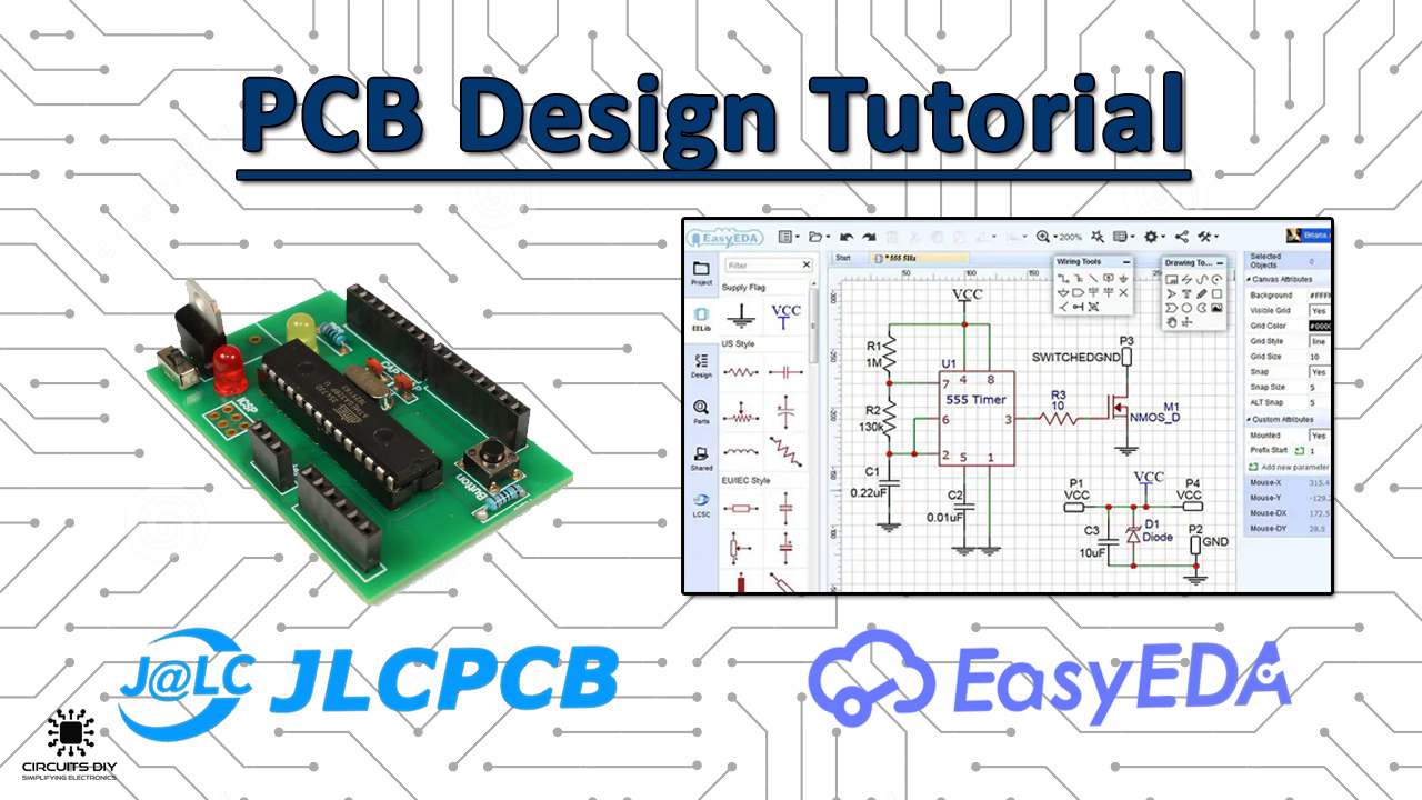
It boasts the same intuitive interface and sleek design as Altium’s professional solutions, making it one of the best PCB software for beginners and hobbyists. It allows you to design with up to 16 signal and 16 plane layers, with no limits on dimensions. You can always etch PCBs at home with a process that’s similar to developing prints from photographic film. It’s much easier (and cheaper) to get your PCB made by a professional manufacturer. To demonstrate the process, I’ll use an online service called EasyEDA to design a PCB layout for an LM386 audio amplifier, then I’ll have it manufactured and show you the results. Their free online design software is easy to use and the rates are very affordable.
Step 3: Synchronize Schematics to Your PCB Board Design
We further demonstrate a non-destructive recycling process based on polymer swelling with small-molecule solvents. Unlike traditional solvolysis recycling, this swelling process does not degrade the materials. Through dynamic mechanical analysis, we find negligible catalyst loss, minimal changes in storage modulus and equivalent polymer backbone composition across multiple recycling cycles. This recycling process achieves 98% polymer recovery, 100% fibre recovery and 91% solvent recovery to create new vPCBs without performance degradation. Overall, this work paves the way for sustainability transitions in the electronics industry.
Manage, Access,and Sync Your Data
Downloading PADS software is easy – simply create an account, visit the download page, select which version you want, click the download button and follow the instructions. You need either Windows 10 or 11 and 8GB RAM to download the program. All the PCB software we’ve reviewed generally offer the same core layout and schematic design features, but the quality varies a lot depending on the program.
Do you work for a PCB Design product?
Solder is the metal that makes the electrical connections between the surface of the PCB and the electronic components. Printed circuit board (PCB) design software is a specialized type of computer-aided design (CAD) software for creating electronic components. These tools are used by engineers to design, test, and optimize PCBs for electronic devices. PCB design software can help engineers produce quality boards efficiently and to a high degree of accuracy.
Too Much Over-optimization Is Never Enough! - Hackaday
Too Much Over-optimization Is Never Enough!.
Posted: Sat, 30 Mar 2024 07:00:00 GMT [source]
When completed, those drawings would be recreated on film using a reduction camera, and that film would be used to make the PCB tooling at the fabrication shop. The PCB designer was as much an artist as they were a budding engineer that needed to master the fundamentals of electrical theory. For the engineer that likes to solve puzzles, create something physical, and appreciates electronics, PCB design as a career might be right for you. Even if you're not a PCB designer or layout engineer, and instead you want to work as an electrical engineer, there is still room for you to work with PCB designers. Today's teams are multifunctional and they need to collaborate across disciplines. It's better to think of electronics development groups as product development teams, where engineers with different types of expertise work together to create a new product.
There’s also a non-profit version that’s 100% free but limited to 500 pins and 2 signal layers, rising to $350 for unlimited functionality. For the full fat version for commercial use with unlimited pins and signal layers, expect to pay around $1000. I ordered 15 PCBs for my LM386 audio amplifier circuit and the cost came out to about $15 USD.

Using the Design Rule Wizard
A PCB is sort of like a layer cake or lasagna- there are alternating layers of different materials which are laminated together with heat and adhesive such that the result is a single object. For example, it’s not uncommon to see offers of 5 copies of your board for less than $5 USD! To design a Printed Circuit Board (PCB), you need to draw holes, pads, and wires for your circuit. 3) Pan by using a Right-drag mouse, or the standard Windows mouse-wheel controls.
Each symbol has a name (R1, R2, C1, C2 etc.) and value (10 μF, 100 Ω, etc.) that can be edited by clicking on the label. Supports high-frequency, high-speed, FPC, and high power PCB design. Easily replace components using the Device Manager, allowing for quick modification of component properties and standardized BOM output. You can easily view all team project status and logs in the workspace. All project data, including projects, libraries, and models, will be owned by the team and can be uploaded as team documents. Data is securely stored on dedicated enterprise servers, enabling support for a larger enterprise user base and ensuring rapid processing and storage of vast amounts of data.
New interface, web-based tool, high efficiency, no need to download. If you have a lot of irons in the fire, we can complete your CAE schematics for you and go directly on to the PCB layout. Strictly Necessary Cookie should be enabled at all times so that we can save your preferences for cookie settings.
Altium's CircuitStudio product is part of a line of PC-based electronics design software for engineers who design printed circuit boards. The first thing you need to check when considering a printed circuit board design software is what operating systems it’s compatible with. For example, if you’re looking for a PCB software for Linux or Mac, you can’t use a program like Altium (which is among the most popular PCB software out there) as it’s only available on Windows.
After you’ve arranged all of the components, it’s time to start drawing the traces. However, they won’t always show you the best way to route the traces, so it’s a good idea to refer back to your schematic to verify the correct connections. The PCB design process follows a standard workflow, and it’s important for any ew designer to understand how this workflow unfolds. The standard workflow in PCB design focuses on taking an engineered design, finishing a physical PCB layout, and preparing the finalized design for manufacturing. Expect to spend around $50 on the board, though it could be lower if it’s not that complex. If you’re letting the manufacturer solder the components as well, you’ll need to pay for each component used.
While continuing to hold down the mouse button, move the mouse to drag the component. 5) Continue placement by clicking on the pause button that is displayed in the center of the schematic. Once the transistor is in the desired position, left mouse click or press Enter on the keyboard to place the transistor onto the schematic. When the blank schematic sheet opens, the main menu bar and related buttons change in context for schematic entry displaying the Active Bar in the workspace.
Perhaps you are already in school and headed for an engineering degree. Or maybe you’re an electronics technician or you are doing some kind of CAD drafting. Maybe you’re not even in the electronics industry, but the idea of mastering printed circuit boards sounds really good to you. If you've wanted to make a career change to becoming a PCB design, or you want to expand your engineering skill set, here's what you can expect.
Altium Designer can save you a substantial amount of time during this PCB design step. Enable accurate design and visualization of HDI structures so you can create layouts with smaller components, tighter traces, and improved performance. Developed by Cadence PCB Solutions, OrCAD is one of the most powerful, reliable, and comprehensive PCB tools on the market and is used by engineers at Apple and other leading companies.


No comments:
Post a Comment